Papers by Alessandro Bramanti
Social Innovation in Long-Term Care Through Digitalization

Nanoscale, Jan 7, 2012
Quantum-dot Cellular Automata (QCA) exploit quantum confinement, tunneling and electrostatic inte... more Quantum-dot Cellular Automata (QCA) exploit quantum confinement, tunneling and electrostatic interaction for transistorless digital computing. Implementation at the molecular scale requires carefully tailored units which must obey several structural and functional constraints, ranging from the capability to confine charge efficiently on different 'quantum-dot centers'-in order to sharply encode the Boolean states-up to the possibility of having their state blanked out upon application of an external signal. In addition, the molecular units must preserve their geometry in the solid state, to interact electrostatically in a controlled way. Here, we present a novel class of organometallic molecules, 6-3,6-bis(1-ethylferrocen)-9H-carbazol-9-yl-6-hexan-1-thiols, which are engineered to satisfy all such crucial requirements at once, as confirmed by electrochemistry and scanning tunneling microscopy measurements, and first principles density functional calculations.
Nanoscale, Jan 7, 2012
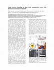
We report on the fabrication and single electron tunneling behaviour of large scale arrays of nan... more We report on the fabrication and single electron tunneling behaviour of large scale arrays of nanogap electrodes bridged by bisferrocene-gold nanoparticle hybrids (BFc-AuNP). Coulomb staircase was observed in the low temperature current-voltage curves measured on the junctions with asymmetric tunnel barriers. On the other hand, junctions with symmetric tunneling barrier exhibited mere nonlinear current voltage characteristics without discrete staircase. The experimental results agreed well with simulations based on the orthodox theory. The junction resistance showed thermally activated conduction behaviour at higher temperature. The overall voltage and temperature dependent results show that the transport behaviour of the large arrays of single particle devices obtained by a facile optical lithography and chemical etching process corresponds with the behaviour of single particle devices fabricated by other techniques like e-beam lithography and mechanical breaking methods.

Most of the current research in nanoelectronics fall into two mainstreams. The first stream attem... more Most of the current research in nanoelectronics fall into two mainstreams. The first stream attempts to transpose the principles of traditional electronics into new technological scenarios. Basically, new ways to build and interconnect transistors are sought for. The second stream is that of research of more innovative solutions tailored on the nanoscale properties of matter, rather than adaptation and reuse old concepts developed at the microscale. In our view, both philosophies fall short of their goal. As to the first, since the transistor has been the very successful elementary brick of electronics for decades, trying to lengthen its life beyond the present constraints of technology obeys a somewhat reasonable economy principle of design. However, molecular-scale transistors generally perform worse than their silicon-based ancestors. Moreover, technologies for interconnecting them into complex, patterned configurations seem far off. The second approach has the merit of looking for a closer linking between the physics of devices and the computational paradigms implemented. The most outstanding and representative topic here is the Quantum-dot Cellular Automata (QCA) paradigm, from which, in fact, this project moves. QCA exploit quantum charge confinement and tunneling, as well as electrostatic interaction, to implement digital computation. Yet, in their original formulation, QCA do not fully account for real world systems, for instance, the cells confining the charges are implicitly supposed to be highly symmetric, as real world molecules are not. And again, no convincing solutions are outlined to pattern computing networks. Overall, realistic post-Moore technologies call for a globally new design style, accounting for physics, technology and computing architecture all at once, so that all the levels (abstract to physical) of the new nanoscale machines are conceived to fit each other. This is just the vision underlying the MolArNet project, which aims to take the fundamental steps toward realistic, out-of-the-lab implementation of molecular QCA.
Nanomaterials, 2022
The widespread use of nanotechnology in different application fields, resulting in the integratio... more The widespread use of nanotechnology in different application fields, resulting in the integration of nanostructures in a plethora of devices, has addressed the research toward novel and easy-to-setup nanofabrication techniques to realize nanostructures with high spatial resolution and reproducibility. Owing to countless applications in molecular electronics, data storage, nanoelectromechanical, and systems for the Internet of Things, in recent decades, the scientific community has focused on developing methods suitable for nanopattern polymers. To this purpose, Atomic Force Microscopy-based nanolithographic techniques are effective methods that are relatively less complex and inexpensive than equally resolute and accurate techniques, such as Electron Beam lithography and Focused Ion Beam lithography. In this work, we propose an evolution of nanoindentation, named Pulse-Atomic Force Microscopy, to obtain continuous structures with a controlled depth profile, either constant or varia...

Nanofabrication, 2011
of Chemistry). 2.2 Top-down processes The top-down approach in building integrated circuits (ICs)... more of Chemistry). 2.2 Top-down processes The top-down approach in building integrated circuits (ICs) usually involves some form of lithography to define the required pattern of features. Many other kinds of processes are required to build an IC, such as ion-implantation, metal evaporation and etching, which are used in several nanoscale devices too; however, here we will concentrate on the problems of lithography, since that is the side of technology directly related to resolution and, consequently, most innovative (and troublesome) in nanodevices. According to a common distinction, we will classify lithographic methods into hard and soft, where the former (often referred to simply as "lithography") are the improved version of those already employed for present ICs, whereas the latter have been purposely developed for nanoscale fabrication (in particular when dealing with fragile molecules). 2.2.1 (Hard) lithography By 'hard lithography' we mean all those techniques using resist layers and optical masks, derived from standard photolithography. The core-idea is to expose a sensitive material (the 'resist') to an activating agent (light or a particle beam) in order to harden (or soften) it in targeted areas. Subsequently, a developer solution will wash away the soft parts of the resist layer selectively, while the remaining hard parts mask the sample for subsequent processing (see the schematic in Figure 2a). Commonly, either the material is etched where unmasked by the layer (and the remaining resist is taken away after the etching); or a new layer of material is grown (e.g. metal by evaporation) so that it builds up upon the patterned resist, where this is present, or upon the underlying material in the resist's voids; finally, the hardened resist will be removed, carrying away the material grown atop (lift-off) and leaving the material inside the patterned voids untouched.
Int. J. Unconv. Comput., 2012

Sensors (Basel, Switzerland), Jan 7, 2018
An accurate and easy-to-use Q3 system for on-chip quantitative real-time Polymerase Chain Reactio... more An accurate and easy-to-use Q3 system for on-chip quantitative real-time Polymerase Chain Reaction (qPCR) is hereby demonstrated, and described in detail. The qPCR reactions take place inside a single-use Lab-on-a-Chip with multiple wells, each with 5 to 15 µL capacity. The same chip hosts a printed metal heater coupled with a calibrated sensor, for rapid and accurate temperature control inside the reaction mixture. The rest of the system is non-disposable and encased in a 7 × 14 × 8.5 (height) cm plastic shell weighing 300 g. Included in the non-disposable part is a fluorescence read-out system featuring up to four channels and a self-contained control and data storage system, interfacing with an external user-friendly software suite. Hereby, we illustrate the engineering details of the Q3 system and benchmark it with seamlessly ported testing protocols, showing that Q3 equals the performance of standard commercial systems. Overall, to the best of our knowledge, this is one of the ...
Smart Materials and Structures, 2017
IEEE Sensors Journal, 2016
Optical Engineering, 2016
Sensors (Basel, Switzerland), Jan 24, 2018
A major trend in biomedical engineering is the development of reliable, self-contained point-of-c... more A major trend in biomedical engineering is the development of reliable, self-contained point-of-care (POC) devices for diagnostics and in-field assays. The new generation of such platforms increasingly addresses the clinical and environmental needs. Moreover, they are becoming more and more integrated with everyday objects, such as smartphones, and their spread among unskilled common people, has the power to improve the quality of life, both in the developed world and in low-resource settings. The future success of these tools will depend on the integration of the relevant key enabling technologies on an industrial scale (microfluidics with microelectronics, highly sensitive detection methods and low-cost materials for easy-to-use tools). Here, recent advances and perspectives will be reviewed across the large spectrum of their applications.
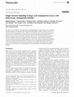
We report on the fabrication and single electron tunneling behaviour of large scale arrays of nan... more We report on the fabrication and single electron tunneling behaviour of large scale arrays of nanogap electrodes bridged by bisferrocene–gold nanoparticle hybrids (BFc–AuNP). Coulomb staircase was observed in the low temperature current–voltage curves measured on the junctions with asymmetric tunnel barriers. On the other hand, junctions with symmetric tunneling barrier exhibited mere nonlinear current voltage characteristics without discrete staircase. The experimental results agreed well with simulations based on the orthodox theory. The junction resistance showed thermally activated conduction behaviour at higher temperature. The overall voltage and temperature dependent results show that the transport behaviour of the large arrays of single particle devices obtained by a facile optical lithography and chemical etching process corresponds with the behaviour of single particle devices fabricated by other techniques like e-beam lithography and mechanical breaking methods.
Uploads
Papers by Alessandro Bramanti
RAI 1 Uno mattina intervista a P. Di Lazzaro e A. Bramanti.