Papers by Bich-Yen Nguyen
IEEE Transactions on Electron Devices, 1994
An advanced, high-performance, quadruple well, quadruple polysilicon BiCMOS technology has been d... more An advanced, high-performance, quadruple well, quadruple polysilicon BiCMOS technology has been developed for fast 16 Mb SRAM's. A split word-line bitcell architecture, using four levels of polysilicon and two self-aligned contacts, achieves a cell area, of 8.61 //liil with conventional I-line lithography and 7.32 pin-with I-line plus phase-shift or with deep UV lithography. The process features PELOX isolation to provide a P. Pelley, photograph and biography not available at time of publication.
Anaerobe, 1997
In this study, the SOI wafers made by various bonding or implant techniques were extensively char... more In this study, the SOI wafers made by various bonding or implant techniques were extensively characterized for physical defects using various metrologies such as optical, X-ray, electron microscopy and SIMS. Defect characterization was performed as received from vendors and after thinning the SOI layer by oxidation and oxide removal
Thin Solid Films, 2004
We describe the use of spectroscopic ellipsometry and other characterization techniques for gate ... more We describe the use of spectroscopic ellipsometry and other characterization techniques for gate oxide process metrology in manufacturing of CMOS transistors for the 130 nm node and beyond. Specifically, we describe the difficulties associated with the introduction of silicon-on-insulator (SOI) substrates, alternative gate dielectrics (silicon oxynitride or metal oxides), and strained Si channels. We predict that spectroscopic ellipsometry by itself will no longer be sufficient for gate oxide metrology, which will make the CMOS gate stack process much more difficult to control. ᮊ
IEEE Electron Device Letters, 2002
We have proposed and simulated a new 10-nm and sub-10 nm n-MOSFET that has a recessed channel and... more We have proposed and simulated a new 10-nm and sub-10 nm n-MOSFET that has a recessed channel and asymmetric source/drain Schottky Contacts (RASC MOSFETs). The recessed channel can effectively suppress short-channel effects, and the asymmetric source/drain contacts in which a higher Schottky barrier at the source contact can yield smaller off-state current while a lower Schottky barrier at the drain
IEEE Transactions on Electron Devices, 2006
A detailed investigation of embedded source/drain SiGe stressors (eSiGes) on a silicon-on-insulat... more A detailed investigation of embedded source/drain SiGe stressors (eSiGes) on a silicon-on-insulator substrate for pMOS performance enhancement is presented. It is found that the integration with undoped SiGe epitaxy suffers strain relaxation from a postepitaxy implantation. SiGe growth with in situ doping is able to retain high strain for carrier mobility enhancement. For doped eSiGe integration with a proper thermal sequence, 20% pMOS drive current improvement is demonstrated. Quantitative analyses of contributions from mobility enhancement and device exterior resistance reduction to the performance improvement are also discussed.
A new CMOS device architecture named as Recessed Asymmetric Schottky Contacted CMOS ( RASC-CMOS) ... more A new CMOS device architecture named as Recessed Asymmetric Schottky Contacted CMOS ( RASC-CMOS) has been proposed and simulated by using commercial version device simulator DESSIS 6.1. RASC-CMOS can eliminate the two critical drawbacks of conventional Schottky contacted CMOS (SC-CMOS): 1) unacceptable off-state current (>10 nA/μm), 2) strong short-channel effects when the feature size of SC-CMOS scaled down to 10 nm. In the meantime, RASC-CM0S has kept the advantage of with extremely simplified fabrication process of SC-CMOS
Journal of Vacuum Science & Technology B: Microelectronics and Nanometer Structures, 2004
SIMS). The crystals obtained have been structurally characterized by X-ray diffraction; the oxyge... more SIMS). The crystals obtained have been structurally characterized by X-ray diffraction; the oxygen content has been determined both by structural examination and by iodometric titration, and the electrical resistivity has been measured by the four-thread technique. SIMS has been used to examine the growth features on the (001) faces of the crystals. Impurity inclusions, ionic species from metals with different oxidation state, homo-and hetero-metal clusters, their ionic yields and distribution in different matrices could usefully be compared to information obtained with traditional methodologies utilized in this field. Results obtained by SIMS for both NdBa 2 Cu 3 O 7À and EuBa 2 Cu 3 O 7À single crystals could provide new instruments in estimating the property of superconducting materials. For example, the reaction of Al-Cu substitution was observed on the crystal surface, as indicated by mixed cluster signals on the positive and negative ion spectra confirming the already observed interaction between material from crucible and REBa 2 Cu 3 O 7À (RE = Rare Earths, except for Ce, Pr and Tb).
A novel method for accurate gate length extraction has been developed using direct tunneling curr... more A novel method for accurate gate length extraction has been developed using direct tunneling current (DTC) through thin gate oxide. Applied to decanano CMOS devices, the proposed method is verified to be free from a severe assumption of unified effective mobility that is one of limitations of conventional method to sub-0.1 /spl mu/m. The DTC method is also insensitive to doping concentration and gate oxide thinning effect at the corner regions. In addition, we have studied the channel length dependence on gate line-edge roughness by comparing the DTC method and the conventional channel current method.
HfO2 is one of the candidates to replace silicon oxide as a gate dielectric for future CMOS techn... more HfO2 is one of the candidates to replace silicon oxide as a gate dielectric for future CMOS technology. Numerous materials requirements must be met to ensure acceptable electrical performance. This paper will present some recent results on materials and physical properties of HfO2 films grown on Si by chemical vapor deposition (CVD) and atomic layer deposition (ALD). Extensive structural, compositional, and optical characterization has been carried out using TEM, AFM, RBS, SIMS, AES, XRD, XPS, and optical spectroscopy (UV-Raman spectroscopy, VUV spectroscopic ellipsometry, and IR transmission spectroscopy). Issues related to impurities, interfacial layers, and thermal stability will be addressed. A new characterization method, tunneling AFM, has also been developed to correlate electrical "hot spots" with film structures.
IEEE Transactions on Nanotechnology, 2003
Page 1. 324 IEEE TRANSACTIONS ON NANOTECHNOLOGY, VOL. 2, NO. 4, DECEMBER 2003 50-nm Fully Deplete... more Page 1. 324 IEEE TRANSACTIONS ON NANOTECHNOLOGY, VOL. 2, NO. 4, DECEMBER 2003 50-nm Fully Depleted SOI CMOS Technology With HfO2 Gate Dielectric and TiN Gate Anne Vandooren, S. Egley, Member, IEEE ...
The electron and hole mobility of Si complementary metal on oxide field effect transistors (CMOS)... more The electron and hole mobility of Si complementary metal on oxide field effect transistors (CMOS) can be enhanced by introducing a biaxial tensile stress in the Si channel. This paper outlines several key analytical techniques needed to investigate such layers. Raman scattering is used to measure the strain in the Si channel as well as to map the spatial distribution of strain in Si at a lateral resolution better than 0.5 μm. Atomic force microscopy (AFM) is used to measure the surface roughness. Transmission electron microscopy (TEM) is used to reveal dislocations in the structure, the nature of the dislocations and the propagation of the dislocations. Secondary ion mass spectrometry (SIMS) is used to monitor the Ge content profile in the structure and the thickness of each layer. In the long term, inline nondestructive techniques are desired for epi-monitoring in manufacturing. Two techniques, spectroscopic ellipsometry (SE) and x-ray reflectivity (XRR), have shown promise at this stage.
Solid-state Electronics, 2004
Raised source/drain (S/D) or raised extension in fully-depleted-SOI (FDSOI) is necessary to boost... more Raised source/drain (S/D) or raised extension in fully-depleted-SOI (FDSOI) is necessary to boost saturation current, because of increased resistance from the very thin film. We demonstrate that the choice of raising the extension versus the S/D, will depend upon the maximum achievable mobility in the structure at a 60 nm physical gate length. We also study the effects of minimum BEOL via spacing on performance, and its consequence on choosing a raised extension or S/D.
Journal of Vacuum Science & Technology B: Microelectronics and Nanometer Structures, 2004
... Xiang-Dong Wang, Chun-li Liu, Aaron Thean, Erika Duda, Ran Liu, Qianghua Xie, Shifeng Lu, Ale... more ... Xiang-Dong Wang, Chun-li Liu, Aaron Thean, Erika Duda, Ran Liu, Qianghua Xie, Shifeng Lu, Alex Barr, Ted White, Bich-yen Nguyen ... MT Currie, CW Leitz, TA Langdo, G. Taraschi, EA Fitzgerald, and D. A Antoniadis, Carrier mobilities and process stability of strained Si n-and p ...

Physica Status Solidi B-basic Solid State Physics, 2003
Strained Si-based technology has imposed a new challenge for understanding dopant implantation an... more Strained Si-based technology has imposed a new challenge for understanding dopant implantation and diffusion in SiGe that is often used as the buffer layer for a strained Si cap layer. In this work, we describe our latest modeling effort investigating the difference in dopant implantation and diffusion between Si and SiGe. A lattice expansion theory was developed to account for the volume change due to Ge in Si and its effect on defect formation enthalpy. The theory predicts that As diffusion in SiGe is enhanced by a factor of ∼10, P diffusion by a factor of ∼2, and B diffusion is retarded by a factor of ∼6, when compared to bulk Si. These predictions are consistent with experiment. Dopant profiles for As, P, and B were simulatedusing process simulators FLOOPS and DIOS. The simulated profiles are in good agreement with experiment. Dopant implantation was simulated using REED-MD. The results showed a noticeable difference in peak and tail positions SiGe compared to Si. (© 2003 WILEY-VCH Verlag GmbH & Co. KGaA, Weinheim)
IEEE Transactions on Nanotechnology, 2003
Page 1. 324 IEEE TRANSACTIONS ON NANOTECHNOLOGY, VOL. 2, NO. 4, DECEMBER 2003 50-nm Fully Deplete... more Page 1. 324 IEEE TRANSACTIONS ON NANOTECHNOLOGY, VOL. 2, NO. 4, DECEMBER 2003 50-nm Fully Depleted SOI CMOS Technology With HfO2 Gate Dielectric and TiN Gate Anne Vandooren, S. Egley, Member, IEEE ...
A low-cost and high-manufacturability Multi-VT Ultra-Thin BOX and Body (UT2B) FDSOI technology is... more A low-cost and high-manufacturability Multi-VT Ultra-Thin BOX and Body (UT2B) FDSOI technology is proposed for high-performance and low-leakage digital circuits. This concept allows setting up low, standard and high threshold voltage (VT) devices without degrading the good channel electrostatic control and the low VT dispersion of the FDSOI technology. Device electrical characteristics, process flow and physical design are described and the performance of digital circuits is evaluated.
IEEE Transactions on Electron Devices, 1994
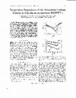
A new analytical model is presented for the temperature and bias dependence of the anomalous leak... more A new analytical model is presented for the temperature and bias dependence of the anomalous leakage current based on thermionic field emission via grain boundary traps in the gate-drain overlap region in polysilicon-on-insulator MOSFET's. The existing model based on pure field emission (tunneling) via grain boundary traps does not include a temperature dependence and therefore cannot explain the observed strong temperature dependence of leakage at low gate voltages, as well as the weaker temperature dependence at high gate voltages, which the new analytical model presented in this paper can. Below 150 K, we believe that impact ionization due to the increasing carrier mean free path leads to the observed increase in the leakage current with decreasing temperature. Since the analytical model does not include impact ionization, it cannot model the leakage current at low temperatures
Continued dimensional scaling of the elements of integrated circuits places significant restricti... more Continued dimensional scaling of the elements of integrated circuits places significant restrictions on the width, density and current carrying capability of metallic interconnects. It is expected that, by the year 2000, the transistor channel length will be at 0.l8piri [1], while microprocessors will pack more than 15 million transistors over an area of '-700mm2. To conserve area, interconnects will continue to be stacked at an increasing number of levels (6 by the year 2000, vs 4 in todays leading microprocessors) and the minimum spacing and width within an interconnect layer will shrink to 0.3.tm. In addition, it is expected that future interconnects will need to sustain increasingly higher current densities without electromigration failures [2]. Aluminum alloys are the conductors of choice in present-day interconnects, and much effort is focused n means to extend the usefulness of aluminum through improvements in reliability, either by new alloy formulations [3], or by the development of complicated multimetal stacks [4. A more radical approach, which is gaining increased attention, is the replacement of aluminum altogether by copper. The bulk resistivity of copper is significantly lower than that of aluminum (1.7.tW-cm for Cu vs. 3.0iW-cm for Al-Cu), which is expected to translate to interconnects of higher performance because of reduction in signal propagation delay. In addition, the significantly higher melting temperature of copper (.-1100°C vs. -600°C for Al-Cu alloys) and its higher atomic weight are expected to translate to improved resistance to electromigration [5]. However, as with any new process trying to break into the mainstream, significant improvement in reliability and performance over that achievable with aluminum alloys must be demonstrated first. Towards this purpose, processes need to be developed that deposit conformal copper films of high purity with acceptable throughput, and integration schemes need to be developed which produce interconnects and multilevel metal structures with reliability significantly better than that of aluminum. This article describes our efforts to integrate copper in the backend of integrated circuits. The first part deals with the chemical vapor deposition (CVD) of copper films. The second describes the integration of copper into the last metal level of a 2-level metal 0.5um BiCMOS SRAM circuit.


Uploads
Papers by Bich-Yen Nguyen