0
\$\begingroup\$

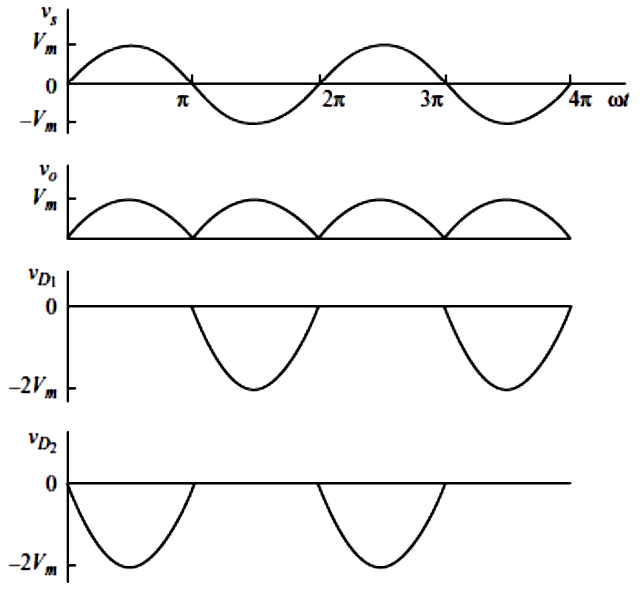
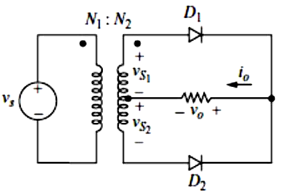
This is a center tapped full wave rectifier. From my understanding if D1 = forward bias and D2 = reverse bias during the positive cycle of AC, why does VD1 from the graph show 0 voltage during the positive cycle and negative voltage during the negative cycle? Shouldn't it be the opposite?

enter image description here

enter image description here

Original Image: https://i.sstatic.net/LF98c.jpg
\$\endgroup\$
0

2 Answers 2

1
\$\begingroup\$

The graph of VD1 shows the voltage across the diode, D1.

  • When VS1 is positive D1 is forward biased. A real silicon diode would have a forward voltage drop of about 0.7 V when current is flowing through it. The graph suggests 0 V drop in the positive direction so they're assuming ideal diodes.
  • When VS1 is negative D1 is reverse biased. It will see the full VS1 voltage across it.

The diagrams are correct.

\$\endgroup\$
1
  • \$\begingroup\$ Took a while to do understand because i only try to look at positive cycle only. thx \$\endgroup\$
    – Ashytone
    Commented Dec 7, 2023 at 13:00
0
\$\begingroup\$

VD1 is the voltage across D1 -- anode relative to cathode. This can never be positive (by more than a small amount), because that would mean that the diode is conducting (forward biased).

In other words, during the first half of the waveform from the transformer, both ends of D1 are following the waveform, and there's no net voltage across the diode.

\$\endgroup\$

Your Answer

By clicking “Post Your Answer”, you agree to our terms of service and acknowledge you have read our privacy policy.

Not the answer you're looking for? Browse other questions tagged or ask your own question.